Effects of Intrinsic Layer Thickness on the Short-Circuit Current Density of Crystalline Silicon-Based Solar Cells
DOI:
https://doi.org/10.19184/cerimre.v2i2.27373Abstract
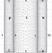
The amount of short-circuits current density (Jsc) shown in the results of the electrical characterization of silicon (c:Si)-based solar cell diodes is one of the determinants of device performance. Efforts to increase Jsc are carried out by adding pure silicon to the diode junction, thereby increasing the magnitude of photoelectron generation in the material. In this paper, the insertion of an intrinsic semiconductor at various thicknesses will be analyzed for its effect on the characteristics of the resulting current-voltage density. By using a 2D simulation based on the finite element method, the solution to the equation of a solar cell semiconductor with a p-i-n junction structure becomes the basis for calculating the resulting electric current density. The thickness variation of the simulated layer i ranges from 1 μm to 15 μm, with a constant thickness of p and n layers of 0.4 m. The simulation results show that the reduced thickness of the intrinsic layer has a significant effect on the decrease in short-circuit current density.